| Fight with the big kid, and you'll get a bloody nose.
That's the message Intel wants to send to rival chipmakers
NexGen, Cyrix, and AMD. Intel's telegram is a massive
next-generation CPU soon to appear in high-end
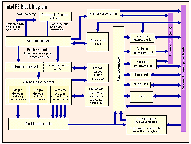
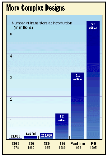
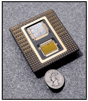
workstations and servers. The new chip has a name: P6. The P6 contains the most transistors ever seen in a mass-market processor. It is aggressively superpipelined, supports out-of-order execution, and has a three-way superscalar microarchitecture. These techniques are impressive but not original — new chips from NexGen and AMD sport similar designs. But Intel has a key advantage: The P6 has a unique secondary cache that is connected to the CPU by a dedicated bus. This 256-KB SRAM (static RAM) cache, which resides in the second compartment of the P6's unusual dual-cavity package, will dramatically simplify the design and construction of systems based on this chip. Intel's estimated benchmarks peg the P6 at about 33 percent faster than a Pentium running at the same clock speed. (The first P6 will run at 133 MHz, which will place it about twice as fast as today's fastest 100-MHz Pentium.) The P6 is thus faster than NexGen's Nx586, which is shipping today, but in the same ballpark as AMD's K5 and Cyrix's M1 — both of which should ship at about the same time as the P6. (For more information, see Intel's new WWW Home Page at http://www.intel.com.) Difficult Questions The P6 is exciting news, but its unveiling also raises a number of serious questions. Is the P6 really a full generation beyond the Pentium? Are Intel's competitors finally catching up? Which CPU is the safest choice for reliability and compatibility? Which is the best buy in terms of price/performance? And looking further ahead, how do these latest CISC chips compare to their RISC counterparts? Will the x86 family remain competitive with such RISC chips as the PowerPC in Apple's Power Mac? Some of these questions can't be answered until more of the competitive x86 chips hit the market. NexGen's Nx586 series has been shipping since last September, but the P6, K5, and M1 are not expected to be available in systems until the second half of this year. Until then, firm pricing and actual system performance are frustrating unknowns. But some questions can be answered today. If Intel's competitors can meet their delivery schedules and performance promises, it appears they have caught up — at least temporarily. Measured against RISC chips, the P6 still isn't the fastest microprocessor you can buy, but it still runs the most software, and it continues to keep the performance gap narrow enough to deny the RISC machines an overriding advantage. The fastest general-purpose RISC processor is Digital Equipment's Alpha 21164, and its integer performance is only about 1.5 times better than the P6's. Another CISC/RISC Hybrid If it's true that great minds think alike, perhaps it's no surprise that the microarchitecture of the P6 resembles those of the Nx586, the K5, and, to a lesser extent, the M1. Engineering teams separated by thousands of miles independently designed each of these x86-compatible processors at roughly the same time. All four combine key elements of RISC technology with some novel concepts to define a bold new generation of CISC. The P6 is obviously Intel's sixth-generation x86, the successor to the Pentium. Until now, the other chips have been considered fifth-generation rivals of the Pentium. But in terms of concept and performance, they are not very different from the P6. This is mostly because Intel's competitors are pursuing their own courses, no longer content to merely clone Intel's designs. By similar but independent routes, they are moving toward the same destination, and the once-discrete generations are starting to overlap. All these processors are 32-bit implementations of the Intel x86 architecture, but their most interesting similarity is the degree to which they adopt the same techniques found in state-of-the-art RISC chips. This is largely because silicon-based microprocessors are a maturing technology, with the easiest gains in performance already behind us. Engineers at all the leading companies are resorting to exotic tricks to squeeze more performance from existing architectures, and even more exotic architectures are taking shape on the drawing boards (see "The P7 and Beyond"). In this respect, the P6 is a significant improvement over the Pentium. Although the Pentium broke ground by introducing the first superscalar x86 microarchitecture, it is a rather pedestrian superscalar design: a pair of integer pipelines that can process two simple instructions in parallel and in order, with no speculative execution. By contrast, the P6 is a three-way superscalar machine that can simultaneously dispatch five instructions internally. To amplify that wider instruction bandwidth, the P6 also has improved caching, more registers, better branch prediction, deep speculative execution, and out-of-order instruction handling. Clearly, it is a design leap beyond the Pentium. It is not, however, a leap beyond its contemporaries. In some cases, the P6 is somewhat more sophisticated than the Nx586, K5, and M1; in other cases, somewhat less. All things considered, the P6's design is on a par with those of the other CPUs, with the K5 its closest relative. Another striking similarity is how the P6, K5, and Nx586 take the same approach to CISC/RISC hybridization. The P6 welds a traditional CISC front end to a RISC-like core, bridging the gap with a clever decoder that breaks down the lengthy CISC instructions into simpler operations that more closely resemble RISC instructions. The simplified operations — Intel calls them micro-ops — are then fed into a core that takes advantage of the latest RISC innovations. Micro-ops are easier to dispatch and execute in parallel than their complex x86 antecedents. NexGen, the newest contender among x86 makers, was actually the first to introduce this idea in an x86 processor. NexGen refers to the simplified operations as RISC86 instructions, and the Nx586 can issue up to four of them simultaneously to its multiple execution units. AMD's K5 has a similar four-way decoder, but the company refers to the simplified instructions as R-ops (RISC operations). Whether you call them micro-ops, RISC86 instructions, or R-ops, the goal of this fission is the same: to overcome the historical limitations of the x86 instruction set while maintaining compatibility with existing x86 software. (Although Cyrix's M1 does not handle x86 instructions in this way, it adopts other RISC techniques to achieve comparable efficiencies.) On the outside — to programmers and the code they write — these processors look like standard x86-compatible CISC chips. On the inside, however, they work much like a modern, streamlined RISC chip. Intel's term for this CISC/RISC hybrid instruction flow is dynamic execution. You'll find the same basic mechanisms if you pry off the lids of the latest RISC processors, including the IBM/Motorola PowerPC 604, the PowerPC 620, the Sun UltraSparc, the Mips R10000, the Digital Alpha 21164, and the Hewlett-Packard PA-8000. Two Chips in One Package The P6's most fascinating feature is a closely coupled secondary (level 2, or L2) cache in the same package with the CPU. Yes, the P6 is two chips in one package. One die is the CPU core, including two 8-KB primary (level 1) caches; the other die is a 256-KB SRAM that functions as the four-way set-associative L2 cache. These two dies share the same 387-pin ceramic package but otherwise are separate wire-bonded chips. Some other companies refer to this type of package as an MCM (multichip module), but Intel is calling it a dual-cavity PGA (pin-grid array). The difference is subtle and probably has more to do with marketing than technology, because MCMs have a reputation for being expensive. (Until Intel announces pricing for the P6 later this year, we won't know if the new terminology will improve that reputation.) No matter what it's called, the P6 is the first microprocessor intended for large-scale production that includes two dies in a single package. The transistor counts are impressive: The CPU die has about 5.5 million transistors, and the L2 die has about 15.5 million. By comparison, the latest Pentium cores have about 3.3 million transistors. Of course, that doesn't include an L2 cache, because as with almost all microprocessors, the Pentium requires an external set of memory chips to implement a secondary cache. If you're wondering why the L2 die in the P6 requires so many transistors for only 256 KB of memory, remember it's SRAM, not DRAM. DRAM chips use only one transistor per bit and are periodically refreshed, and SRAM chips use four or six transistors per bit so that they don't need refreshing. That's what makes SRAM faster and more expensive than DRAM. The SRAM in the P6 has six transistors per bit. Although the L2 die in the P6 has about three times as many transistors as the CPU die, the CPU die is physically larger. It measures 306 millimeters square (compared to 295 for the first Pentium), while the L2 die is only 202 mm square. Both are fabricated on the same process (0.6-micron, four-layer metal BiCMOS), but it's easier to pack transistors more densely onto memory components than onto logic parts. Here's why Intel incurs the extra expense of packaging the CPU core and secondary cache together: First, the combination package will make it easier for vendors to design high-performance systems around the P6. One challenge of designing a computer with a fast processor is fine-tuning the size and configuration of the secondary cache to the requirements of the CPU. Unfortunately, the low margins of today's PC-clone market do not encourage lavish R&D budgets. At the same time, clone vendors are under great pressure to get their machines out the door as soon as possible. The P6's built-in secondary cache is already tuned to the CPU and will let systems designers quickly integrate the package onto motherboards. Another important reason for the dual packaging is enhanced performance. The secondary cache is closely coupled to the CPU core by a dedicated bus that is 64 bits wide and runs at the same speed as the CPU clock. If the CPU core is clocked at 133 MHz (at which speed the P6 will debut), the secondary cache also runs at 133 MHz. The first Pentiums were clocked at 60 and 66 MHz, and they addressed their secondary cache over a 64-bit bus that ran at the full speed of the CPU core. However, as Pentium clock speeds increased, it became too difficult and expensive for systems designers to match those speeds on their motherboards. So the faster Pentiums use a clock divider to run the external bus at a fractional speed. For example, a 100-MHz Pentium runs its external bus at 66 MHz, and a 90-MHz Pentium runs its external bus at 60 MHz. The Pentium also uses this same bus to access main memory and other peripherals, such as the PCI chip set. Because the P6 has a dedicated bus for the secondary cache, it achieves two efficiencies: full synchronous bus speeds and no contentions with other I/O operations. The dedicated L2 bus, or backside bus, is completely separate from the external I/O bus, or frontside bus, so the P6's secondary cache doesn't have to share access with main memory and peripherals. The 64-bit frontside bus can run at one-half, one-third, or one-quarter the speed of the P6's core, depending on the wishes of the systems designer, and the backside bus continues to run independently at full speed. These are big improvements over the bus designs of the Pentium and most other x86 processors. However, NexGen was there first with a similar design. Although the Nx586 doesn't package the secondary cache with the CPU, it does integrate an L2 cache controller and a full-speed backside bus. Like the P6, the Nx586 accesses main memory and peripherals concurrently over a separate I/O bus that runs at a clock-divided frequency. Digital's Alpha 21164, an exotic RISC chip, goes a step further by integrating a 96-KB secondary cache with the CPU core, just like a primary cache. This provides unprecedented cache performance at the expense of considerable silicon real estate — the Alpha 21164 contains a whopping 9.3 million transistors, most of which are arrayed in the caches. The payoff is that the Alpha 21164 delivers 330 SPECint92 at 300 MHz. Intel's P6 isn't quite that fast (Intel estimates 200 SPECint92 at 133 MHz), but it strikes a better balance between speed and cost for its intended market. One caveat: The P6's unusual design will make it difficult to calculate its price/performance ratio, even when we know the price. The built-in secondary cache is bound to make the P6 look more expensive than its competitors, but most of the other processors require an external set of memory chips, as well as a cache controller. The more efficient design of the P6's cache structure means the other processors will probably need more than 256-KB cache to achieve comparable performance. Keep those factors in mind when evaluating systems. Intel's unique packaging also leaves the door open for more design variations. Future versions of the P6 could easily enlarge the secondary cache or take the more conventional approach of separating the cache from the package. A P6 with an external secondary cache wouldn't be pin-compatible with a multichip version because it would require 72 more pins (64 for the backside bus and eight for error-correction coding), but it would be just as fast, especially when burst-mode SRAMs become available. History shows that Intel likes to offer numerous variations of a basic processor design. It provides more flexibility for system vendors and leaves less room for competitors to carve out market niches. One variation that wouldn't make sense, according to Intel, is to connect an external set of memory chips to the P6's frontside bus to implement a level 3 cache. The Alpha 21164 is designed to work with an L3 cache, but Intel says it wouldn't buy much performance for the P6 because the L1 and L2 caches already are closely matched to the demands of the core. P6 Microarchitecture Modern microprocessor design requires careful attention to balancing all the different elements in the chip. It's not just a matter of adding more resources in the form of larger caches, wider buses, faster clocks, multiple execution units, and additional registers, because some of those resources will be wasted if they exceed the ability of others to keep up. Intel started designing the P6 about four years ago (roughly halfway into the Pentium's design cycle), and the Oregon-based engineers spent much of that time fiddling with simulators to determine the optimum combination of I/O bandwidth and execution capacity. The closely coupled secondary cache is only one example of how Intel boosted the P6's bandwidth to feed the hungrier appetite of its superscalar core. Another example is how Intel made the primary and secondary caches nonblocking without increasing their size. Each cache in the P6 is 8 KB; the instruction cache is two-way set-associative, and the data cache is four-way set-associative. The Pentium also has a pair of 8-KB primary caches, although both are two-way set-associative. Normally, you would expect to find larger primary caches (and a larger secondary cache) in a three-way superscalar machine like the P6. Instead, Intel has designed the cache hierarchy to allow requests to flow from one cache to the other without blocking execution. If the P6 cannot find the instructions or data it needs in the primary caches, it quickly checks the secondary cache. Thanks to the backside bus, the penalty is only one clock cycle. If the P6 can't find what it needs there, it must access main memory over the frontside bus. The penalty for a double cache miss is usually considerable, because the frontside bus runs at a divided clock speed and main memory is relatively slow. But Intel has taken steps to minimize the impact. First, as described above, the independent frontside and backside buses operate concurrently. Second, the frontside bus is transactional, another improvement over the Pentium. While the P6 is waiting for a memory access to complete, it can begin another access. As many as eight of these transactions can be outstanding. Transactions can be loads or stores, and each transaction is recorded in a MOB (memory order buffer) so that the CPU won't mix them up. In fact, the P6 can let a load "pass" a pending store, which greatly accelerates throughput. While a Pentium would stall in this situation, the P6 can continue issuing loads and stores and execute other nondependent instructions that are queued in its buffers. To maintain coherency between the caches and memory, the P6 implements the MESI (modified, exclusive, shared, invalid) coherency protocol. This guarantees cache coherency in both single- and multiprocessing systems, and it also guards against potential tragedies caused by self-modifying code. Many old x86 programs (and even some naughty new ones) use this technique, which can wreak havoc when the program rewrites portions of itself that are already cached. The P6 detects this, and even dedicates a machine-specific register to track how often it happens. An operating system could check this register and warn you if your programs are too clever for their own good. The combination of nonblocking caches, separate fetch buses, and an eight-entry transactional buffer goes a long way toward ensuring that the P6's multiple execution units won't run out of work to do. Instruction Fission One of the historical burdens of the 17-year-old x86 architecture is its complex instruction set. In the late 1970s, when Intel engineers were designing the original 8086, the goal was to pack the richest possible instruction set onto a chip with only 29,000 transistors. They did it by creating complex instructions that do a lot and require microcode. But as processors grew more powerful, those long, complex instructions became a liability. RISC processors take the opposite tack by using instructions that are relatively simple and are hard-wired onto the chip. RISC instructions are easier to handle internally, especially in a superscalar machine, so the trend in CISC design is to make the complex instructions appear more RISC-like without changing them. Changing the CISC instructions is unthinkable because it would render existing software obsolete. The approach introduced by NexGen and adopted by AMD and Intel is to build an x86 preprocessor with a sophisticated decoder that parses the complex instructions into fragments of simpler operations: These are the RISC86 instructions, R-ops, or micro-ops mentioned before. The simplified operations are easier to dispatch and execute in parallel than full-length x86 instructions. Instruction fission begins soon after the x86 instructions are fetched into the pipeline. Interestingly, the P6 adopts another RISC technique at this point that the latest RISC chips are retreating from: superpipelining. The P6 has a 14-stage pipeline (although in some instances stages can overlap), considerably longer than the Pentium's five-stage pipeline. (Due to the complex nature of the x86, some instructions consume additional pipeline stages, and floating-point instructions may require many more stages.) Superpipelining is falling out of favor with some engineers because it can impose costlier penalties when the CPU misses the cache or mispredicts a branch. Intel is trading off those disadvantages against faster overall throughput, because the P6's stages have shorter latencies than the Pentium's, and they help to keep the execution units busy. The first stage of this superpipeline calculates the next value of the instruction pointer, which determines the location from which the CPU will fetch the next instruction. This calculation isn't as simple as merely incrementing the pointer, of course, because there might be a pending interrupt or a branch that would move the pointer to a different location. During the next three stages, the P6 fetches two cache lines of 32 bytes each, marks the boundaries of each instruction, and passes 16 aligned bytes to the decoder. Two cache lines are fetched per clock because x86 instructions can be long, so there's a good chance an instruction will wrap around from one cache line to another. Marking the boundaries is important because x86 instructions vary in length (8 to 120 bits), so it's not obvious where one instruction ends and the next begins. (RISC instructions are easier to fetch because they're always 32 bits long.) The following stages of the P6's pipeline are noticeably different from the Pentium's. Instead of merely decoding the x86 instructions and shoving them down a pair of execution pipelines, the P6 converts them into sequences of micro-ops and appends various flags and status bits to prepare them for superscalar out-of-order issue. To do this, the P6 has a decoder unit that is much more sophisticated than the Pentium's; it actually consists of three decoders working in parallel. Two of these decoders parse the simpler x86 instructions, mostly integer operations. When they encounter a more complicated x86 instruction, they pass it along to a more sophisticated third decoder. Some instructions are too complex for even this decoder to parse, so they're referred to a microcode instruction sequencer, which corresponds to the microcode ROM in earlier x86 chips. In any case, the final output is the same: triadic micro-ops that always contain three operands — two sources plus a destination. They're longer than true RISC instructions because they have to accommodate the more complex x86 floating-point operations, but they're definitely easier to manage than the original x86 instructions from which they are derived. Most x86 instructions map directly into single micro-ops. All but the most complex instructions translate into one to four micro-ops. When an instruction is so complex that it must be broken into more than four micro-ops, it is passed to the microcode instruction sequencer. The worst-case situation is difficult to pin down because x86 instructions can have prefixes that greatly multiply their complexity. However, if the instruction doesn't have a repeat prefix, isn't looped, and isn't a string operation, the worst case is that it will translate into 204 micro-ops. The two simpler decoders in this mechanism can each generate one micro-op per clock cycle. The third decoder can generate up to four micro-ops per clock cycle. Therefore, with each clock cycle, the unit can churn out as many as six micro-ops. That's better than the similar decoders in the Nx586 and K5 processors, which can generate a maximum of only four RISC86 instructions or R-ops per clock cycle, respectively. Although Intel's micro-ops are comparable to an internal RISC-like instruction set, Intel says the P6 does not allow external access to the micro-ops. In other words, you can't write or compile a program in micro-ops and run it faster on the P6 by circumventing the decoder. The K5 has no provision for this, either. The Nx586 does permit such a bypass, although it's unlikely it will ever be used for anything but in-house testing by NexGen engineers. If Intel permitted this on the P6, it would raise the spectre of a new generation of software that discarded the troublesome x86 instruction set altogether. After the decoder converts the x86 instructions into micro-ops, stages 7 and 8 finish preparing them for superscalar issue. In stage 7, references to x86 logical registers are reassigned to physical registers by the RAT (register alias table). This is similar to the register renaming found in other advanced microprocessors and is yet another way in which the P6 overcomes a historical limitation of the x86 architecture. Ever since the 8086, the x86 architecture has made only eight integer-type GPRs (general-purpose registers) visible to programmers. That's a small register file in modern terms, but Intel can't expand the number of architectural GPRs without disrupting the x86 standard. Register renaming solves that problem by adding more physical registers to the chip and renaming them on the fly to represent logical (architectural) registers. In other words, at any given moment, any of the physical registers in the expanded register file can represent the logical registers that x86 programs expect to see. The P6 has an impressive total of 40 extra GPRs, in addition to the architectural set of eight integer and eight floating-point GPRs. By comparison, the M1 has a total of 32 GPRs, the K5 has 16, and the Nx586 has 14. The P6's expanded register file allows the CPU to explore more deeply when it speculates beyond predicted branches. Furthermore, the 40 extra GPRs in the P6 are wide enough to handle floating-point values and integer values, as well as some additional status information that's appended in stage 8. The expanded register file functions as a general-purpose instruction pool that Intel calls an ROB (reorder buffer). This ROB is a 40-entry array of content-addressable memory that's arranged as a circular FIFO (first in, first out) buffer. Micro-ops (now a uniform 118 bits long) are held in this pool during various states of completion. Status bits record the state of each micro-op and provide additional information, such as which execution unit can handle that type of micro-op. Deliberate Disorder Until this point, the P6 has been processing the instructions in their original program order, just like the Pentium and earlier x86 chips. But this is where the P6 differs radically from the Pentium. In-order CPUs frequently stall while they wait for a time-consuming instruction to complete. Because they must execute the instructions in the same order as they're arranged in the program, any instruction that causes a delay interferes with the smooth throughput of the pipeline — just as a factory assembly line halts when one worker takes too long to finish his task. To prevent this wasteful idling, the latest CPUs can execute instructions in almost any order they choose. Instead of waiting around for a poky instruction to complete, the CPU can fetch and execute a following instruction. Of course, to avert a software disaster, the CPU eventually stores the results in the order the programmer intended. Some sequences of instructions must always execute in order because one instruction depends on the result of a previous instruction. This is called a true dependency, and the P6 is careful not to mix up these sequences. Among the status bits appended to each micro-op is a dependency flag and a time stamp that records the micro-op's original position in the instruction stream. Out-of-order execution is a vital feature of the P6, Nx586, K5, M1, and many RISC chips. When combined with branch prediction and speculative execution, it allows the CPU to adapt the instruction stream to the availability of its internal resources. In effect, the CPU is its own optimized compiler. As long as there are no dependencies, the CPU can continue predicting the outcome of branches and speculatively execute the instructions beyond those branches. There's no absolute limit to how far ahead the P6 can speculate, other than the capacities of its ROB, execution units, and other resources. Intel says the P6 typically looks 20 to 30 instructions beyond the program counter. Branch prediction plays an important role in this process because the average program contains one branch every five instructions. (If you're a programmer and you're wondering why your own programs don't contain that many IF...THEN statements, remember that loop terminations and other statements compile into branches, too.) To reduce this number somewhat, the P6 adds one new instruction to the x86 instruction set: A conditional MOV that in some cases replaces a regular branch. When a branch instruction enters the ROB, it is tagged with extra status bits that indicate a predicted target address and a fall-through address. Actual target addresses are stored in a 512-entry BTB (branch target buffer). The target address determines which cache lines will be retrieved during the next fetch cycle. Using a 4-bit dynamic history algorithm, the BTB keeps track of whether the branch was correctly predicted. This algorithm is smart enough to recognize patterns (e.g., alternating pairs of taken/not-taken branches) that would baffle some simpler algorithms, such as the binary flip-flop used by the K5. According to Intel, the P6's branch prediction is more than 90 percent accurate. Thanks to its large BTB and ROB, the P6 typically predicts 10 to 15 nested branches, which is impressive indeed. Even some of the latest and most powerful RISC chips, such as the Mips R10000, can go only four branches deep. But what happens if the P6 guesses wrong? This is when superpipelining works against the P6. A mispredicted branch can invalidate all the work in progress in previous pipeline stages — all the speculated instructions (and nested branches) beyond the mispredicted branch. The P6 must discard numerous entries in the BTB and the ROB. The emptied stages cause pipeline "bubbles" that impair the CPU's throughput until they are replenished. There are two ways to measure the cost of a mispredicted branch: the actual loss of clock cycles required to recover from the wrong guess and the potential loss of work that was done speculatively and must be abandoned. For instance, say you're playing roulette and bet a dollar on number 18. There's a 36-to-1 payoff if you win. But if you guess wrong, how much money have you lost? Your actual loss is the $1 you wagered, but your potential loss is the $36 you could have won by guessing right. Similarly, the P6 pays two penalties for guessing wrong. Intel says the actual penalty is usually eight clock cycles, the time it takes to update the various buffers and registers, redirect the instruction pointer, and refill the pipeline. (A hinting mechanism can reduce this to four clock cycles.) The potential penalty is more variable and depends on how many instructions were speculatively executed past the mispredicted branch. Because the P6 looks far ahead, this can easily be 20 or 30 instructions. Intel says the P6, unlike the Pentium, is designed to deliver more of its potential speed without requiring optimized code. Nevertheless, there's no question that any compiler optimizations that minimize branches or enhance the CPU's ability to predict branches will boost performance — for all advanced CPUs, not just the P6. Intel says it is working with software vendors to develop post-compilation code profilers that will squeeze a little more speed out of the chips. Superscalar Execution Out-of-order execution in the P6 is managed by a unit called the reservation station, which is similar to the reservation stations in the K5 and the PowerPC. The reservation station is like a traffic cop; it's responsible for scheduling the order in which the micro-ops are dispatched from the ROB to the multiple execution units. There are five execution units: two IUs (integer units), two AGUs (address-generation units) for load/store operations, and an FPU. The reservation station can dispatch up to five micro-ops to these units per clock cycle, but a sustained rate of three per clock cycle is more likely because some of the units are usually busy. To schedule this dispatching, the reservation station checks the status bits of the micro-ops waiting in the ROB. If the micro-op isn't locked by a dependency, its operands are ready, and an execution unit that can handle that type of micro-op is available, then the reservation station dispatches it for execution. If more than one micro-op is ready for dispatching, the reservation station picks those that were generated in sequence. Although this pseudo-FIFO algorithm favors in-order execution, by now the instruction stream has become so rearranged by dependencies and branches that it's substantially out of order. These steps occupy stages 9 and 10 in the pipeline, although in many cases stages 8 and 9 overlap. The next stage, execution, may consist of many stages if the micro-op is a relatively complex operation (e.g., a floating-point operation). Over the years, however, x86 processors have added much hard-wired logic, so the majority of integer operations (which make up most of the instructions in typical programs) execute in a single clock cycle, just like RISC instructions. Modern x86 compilers try to use as many of these fast instructions as possible. To boost floating-point performance, the P6 has the same beefed-up FPU found in the Pentium, which means there is additional logic to handle multiply, divide, and shift operations. It's undoubtedly the fastest FPU on any x86 processor, even though it still falls well short of most RISC chips. Incidentally, the P6's FPU is free of the division bug that afflicts the Pentium. In fact, the FDIV bug was confirmed when Intel engineers testing the P6's FPU discovered that the P6's output matched that of the 486, but not the output of the Pentium. Load and store operations in the P6 require one and two micro-ops, respectively. A load operation needs to know only the memory location and the width of the data, so it's only one micro-op. A store must generate the memory address and the data; the decoder breaks the operation into two micro-ops so that they can execute in parallel. In fact, the AGU that handles stores has two ports and is separate from the load AGU, so the reservation station can dispatch a load and a store on the same clock cycle. The P6 tries to maximize parallelism by spreading the execution units across five different ports on the reservation station. The two AGUs do not share the same ports, and neither do the two IUs. The FPU shares a port with one of the IUs, but because the FPU has such long latencies (due to the complexity of its operations), it rarely blocks the IU. Time to Retire After a micro-op has executed, its status flag is changed to indicate completion, and it is returned to the ROB. Thus, the ROB is a generalized pool for micro-ops that are awaiting either execution or retirement. Both the reservation station and the retire unit constantly scan this pool, looking for micro-ops with the appropriate status flags. When the retire unit finds a completed micro-op, it verifies that the micro-op can indeed be retired. This is not as easy as it sounds, because the retire unit must put the micro-ops back into their original program order and watch for interrupts, traps, faults, breakpoints, and mispredicted branches. For example, an interrupt could invalidate any micro-ops that were completed speculatively after the one that was interrupted. The P6 supports precise exception handling to the extent that the x86 architecture does, which means some instructions can be interrupted in midstream. If a micro-op is ready for bed, the retire unit stores the results. This is when physical state is committed to logical state. If the original x86 instruction from which the micro-op is descended stores a result in a logical register, then the retire unit copies the result from the physical register that holds that value to the appropriate logical register. Intel refers to the logical register set as the RRF (retirement register file), but it's really just the architectural set of eight integer and eight floating-point GPRs found in any x86 chip. If the result of this retirement affects the status of another micro-op waiting in the ROB, the buffer is updated as well. These steps occupy stages 12, 13, and 14 in the pipeline, although the last execution stage overlaps the first retirement stage. Retirement therefore takes two clock cycles, and the retire unit can commit the results of up to three micro-ops per clock cycle. In other words, the P6 is a three-way superscalar machine. The K5 is four-way superscalar, and the M1 is a two-way superscalar, like the Pentium, only more efficient. The Nx586 is harder to categorize because it can issue three or four RISC86 instructions simultaneously, depending on whether the optional FPU is present. Ultimately, the final test of these competing microprocessors will be their performance when running everyday applications in typical systems. If the K5 and M1 live up to their promises, they should run neck and neck with the P6. The P6 and K5 appear to have more headroom for improved performance than do the M1 and the Nx586, but all four processors belong to roughly the same x86 generation — whether you call it five-and-a-half or six. Intel commands such a dominant market share that it's unlikely the P6 will ever be seriously threatened by its rivals. And the P6 does a creditable job of defending Intel's technical leadership. But it's now clear that AMD, Cyrix, and NexGen no longer lag four or more years behind Intel with derivative clone designs. A new age has dawned, and users are the winners. Sidebars:
The P6: What's New
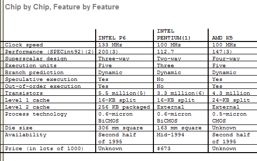
Chip by Chip, Feature by Feature
[1] P54C Pentium at 100 MHz. [2] Benchmark suite revised November 1994. [3] Estimated performance. [4] Not including optional FPU. [5] Packaged level 2 cache has 15.5 million transistors. [6] Pentium-60 and -66 have 3.1 million transistors. [7] Integrated level 2 cache controller. [8] NexGen plans die shrink to 119 mm square in April. 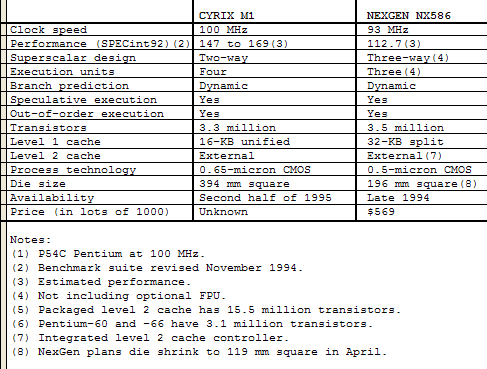
Tom R. Halfhill is a BYTE senior news editor based in San Mateo, California. You can reach him on the Internet or BIX at thalfhill@bix.com. Letters / June 1995Intel's P6I enjoyed your article "Intel's P6" (April); however, the P6 is not the first chip "intended for large-scale production" with two dies on a single package. That honor goes to the DEC J-11 11/70-on-chip. The J-11 was the first PDP-11 (maybe the first chip of any type) to be able to do register-to-register instructions in one cycle (200 nanoseconds), and it had a four-level pipeline, truly great accomplishments in 1982. Bob Morris President DSPS Digital Signal Processing, Inc. Carleton University Ottawa, Ontario morris@sce.carleton.ca I really enjoy the depth to which BYTE explores topics like the P6. I still have a few questions regarding your April Cover Story. On what front-end bus speed (1/2 CPU, 1/3 CPU....) does Intel base the P6's performance numbers? Also, I was under the impression that a 100-MHz Pentium really runs at 99 MHz. This would make it easy to use a PLL (phase-locked loop) to create 66 MHz for the main bus. It follows that the P6 would use a 132-MHz clock rate so the main bus would run at 66 or 33 MHz. Karl Richards richardk@execpc.com The P6's I/O (i.e., frontside) bus can be clocked at 1/2, 1/3, or 1/4 of the core speed. The performance estimates from Intel are based on a system that runs internally at 133 MHz and externally at 66 MHz. In other words, 1/2 clock speed. It doesn't make sense to run a 133-MHz P6 at 1/3 or 1/4 — those dividers were included for future P6 chips that will run at faster core speeds. My understanding is that a 100-MHz Pentium actually runs at 100 MHz, not 99 MHz, and that a 133-MHz P6 runs at 133 MHz, not 132 MHz. — Tom R. Halfhill In your April Cover Story you describe the physical dimensions of the current crop of processor chips as "306 mm square." That comes very close to being a foot on a side. We'll have to redesign all our personal computers just to hold the CPU. This is too much! Merritt J. Rucher Belen, NM Yes, the size was supposed to be written as "square millimeters," not "millimeters square," but somehow it got transposed . — Tom R. Halfhill Letters / July 1995P6 Pointers?I read your cover story entitled "Intel's P6" (April) and was hoping to get some additional references from you. The only information I've been able to find on the P6 is in your article and in Intel's home page. Mark Brehob East Lansing, MI As far as I know, my story on the Intel P6 is the most detailed information available in a general magazine. The only source for more information is the February 16 issue of Microprocessor Report, a newsletter that covers the semiconductor industry. It's not available on newsstands, and subscriptions cost $495 a year. Intel will eventually publish a manual on the P6, but it's not available yet, either. — Tom Halfhill Copyright 1994-1998 BYTE |